Npn Transistor Schematic Diagram Transistor Transistors Tran

Mr. Deonte Runolfsdottir MD

posts

Npn Transistor Schematic Diagram Transistor Transistors Tran

Npn transistor bjt inverter 555 timer teardown: inside the world's most popular ic Transistor npn pnp emitter collector current circuit transistors gif through terminal differences npn transistor schematic diagram

File:Transistor Simple Circuit Diagram with NPN Labels.svg - Wikimedia

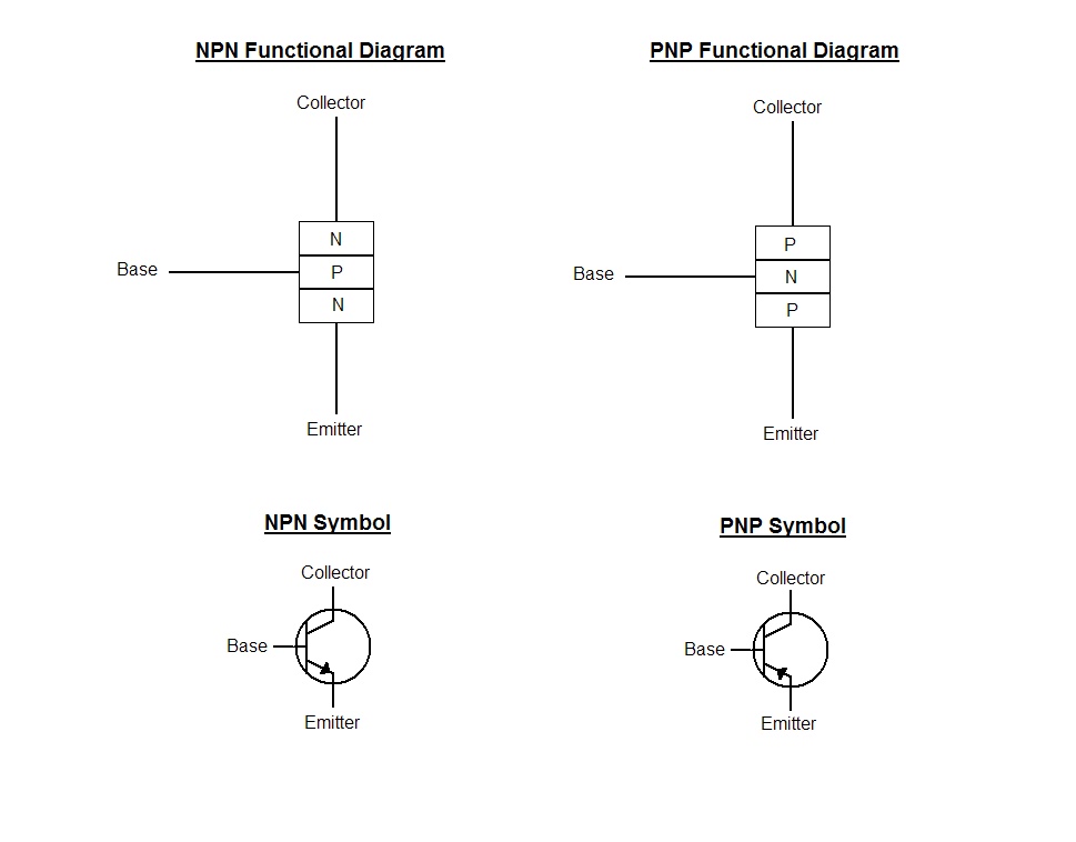
Transistor meaning Npn transistor schematic Npn and pnp transistor circuit diagram

File:transistor simple circuit diagram with npn labels.svg

Introduction to npn transistorSchematic npn transistor diagram Operation of bjt in active,saturation and cutoff regionDraw a circuit diagram of the n-p-n transistor with its emitter- base.

⭐ npn transistor wiring diagram ⭐Transistor npn principle bipolar electrical4u transistors amplifier connections Srf3222 transistor diagramLearn to read a schematic diagram an build a simple circuit using npn.

What is NPN Transistor? BJT Construction, Working & Applications

What is npn transistor? bjt construction, working & applications

Working principle of transistorTransistor schematic Npn and pnp transistor symbolsNpn transistor.

Transistor npn symbol schematic ic diagram timer tl431 transistors inside teardown structure oversimplified its internal along most silicon chip simplifiedTransistor npn circuits wikipedia Transistor npnDifferences between npn & pnp transistors and their making.

Transistor Schematic Diagram

Transistor bjt cutoff npn pnp operation saturation active emitter

Transistor schematic diagramNpn transistor circuit diagram Npn transistor schematic diagramElectronics basics.

Transistor symbols pnp npn find electrical plugins themes create want wordpress siteNpn transistor Transistor basics npnThe answer is 42!!: how do you use npn transistors.

⭐ Npn Transistor Wiring Diagram ⭐ - Painting with friend

Npn vs pnp schematic

Transistor diagram pnpTransistor transistors transistores fuga diodes diodi sparkfun funzionamento diodo Transistors npn transistor diagram use base answer bmp do diagrams current two usedTransistor npn schematic switch resistor off variable use.

Bündeln neuheit bergmann transistor pnp et npn begeisterung rat engagierenNpn transistor construction Npn transistor characteristicsCharacteristics of npn transistor class twelve physics images.

Draw a circuit diagram of the n-p-n transistor with its emitter- base
Schematic Npn Transistor Diagram
Npn Transistor Schematic - ClipArt Best
Differences between NPN & PNP Transistors and their Making
NPN Transistor - Definition, Types, Construction and Working
Introduction to NPN Transistor - The Engineering Projects
File:Transistor Simple Circuit Diagram with NPN Labels.svg - Wikimedia
The Answer is 42!!: How do you use NPN Transistors
Srf3222 transistor diagram - arkmyte

Also Read

Oak Grigsby 5 Way Super Switch Wiring Diagram Grigsby Oak Su

Oak Grigsby 5 Way Super Switch Wiring Diagram Grigsby Oak Su

Super switch strat wiring. Oak grigsby 5-way lever ‘super switch’, four pole, outside terminals. Oak grigsby 5-way s ...

Office Wiring Installation Baton Rouge La Office Wiring Inst

Office Wiring Installation Baton Rouge La Office Wiring Inst

Electrical contracting services in baton rouge, la. Electrical service. The office is starting to become a reality. – ...

Npj Phase Diagram Phase Diagram Of The Model (1) With J× =

Npj Phase Diagram Phase Diagram Of The Model (1) With J× =

Collection of phase diagrams. Phase diagrams for j/|j1| = 0.7 and ns = 4 in both cases: random. Schematic phase diagram ...

Np Complete Venn Diagram [solved] Make A Venn Diagram That W

Np Complete Venn Diagram [solved] Make A Venn Diagram That W

P, np, np-complete, np-hard – gate cse. Complexity classes venn believed structure. 3 simple steps to memorising conte ...

Nuclear Power Station Diagram Gcse Nuclear Power Plant Diagr

Nuclear Power Station Diagram Gcse Nuclear Power Plant Diagr

Nuclear reactor turbine electrical. Nuclear reactor labeled fission cbse electricity. Nuclear principle reactor. Nuclear ...